|
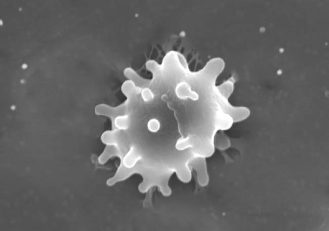
Scanning
Electron Microscope (SEM) image of a White Blood Cell
SEM stands for Scanning Electron
Microscope. The term "SEM" is used to describe a microscope used to
create high magnification, black and white images of devices with
dimensions from a few tenths of a
micron to several millimeters in diameter.
The term SEM is also used to describe the photographs taken by the
Scanning Electron Microscope. Hence, SEM refers both to the microscope,
and the photograph created by the microscope.
Traditional optical microscopes have a
very shallow depth of field. This means that images created with optical
microscopes have only a small area that is in focus. Optical microscopes
can create quality images of things that are flat, but can not create
good images of three dimensional structures because of the focus issues.
Scanning Electron Microscopes, on the other hand, have a very large
depth of field. This means that they can image complex three dimensional
structures, with all parts of the device being imaged being in focus.
This large depth of field results in stunning, sharp photographs of very
small things.
|
|
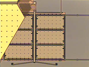
SEMs are only able to create Black and
White images. When SEM images are used in publications or books, they
are sometimes colored by a graphic artist for dramatic impact. It should
be understood, however, that the colors were added by an artist, and in
no way reflect the actual structure being depicted. Optical microscopes,
on the other hand, can create true color images. In comparing the two
photographs above, it can be seen that the SEM creates much sharper
images than what can be achieved with an optical microscope. The
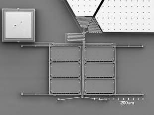
two structures pictured above are
MEMS (MicroElectroMechanical System)
devices. These devices are relatively flat. The advantage of the SEM
becomes more pronounced as devices become more three dimensional.
A scanning electron microscope operates
by using a beam of electrons to image extremely small structures. The
electron beam is created by a cathode typically made of tungsten. An
electric field is used to accelerate the electron beam towards the
cathode, where the structure to be imaged is located. Coils or deflector
plates are used to scan the beam across the sample to be imaged. The
resolution that can be achieved depends on the spot size of the electron
beam. The smaller the beam, the better the resolution that can be
achieved.
In order to achieve proper creation,
control, and detection of the electron beam, the imaging must be done in
a vacuum. In addition, in order to get good contrast and resolution, the
surface of the device to be imaged must be very conductive. These
requirements of conductive surfaces, and operation in a vacuum requires
that a sample be properly prepared in order to achieve good images.
Biological samples can be damaged when placed in a vacuum, as the water
in the sample will vaporizes, which can cause the sample to explode or
dehydrate.
A typical sample preparation for
non-conductive solids, and biological samples is to coat the sample with
gold prior to imaging. A very thin coating of gold will provide the
conductivity needed, and will offer protection for fragile biological
material. The images presented on this site were all created by
first gold coating the samples.
More recently, a new type of SEM has been
developed which does not require high levels of vacuum. These
environmental SEMS allow imaging of devices which can not be coated with
gold, or prepared with other techniques. Environmental SEMS offer the
ability to image structures which previously were not compatible with
SEM imaging. The resolution and contrast of images in an environmental
SEM are typically not as good as a traditional SEM.
|